US7107568B2 - System and method for reducing wire delay or congestion during synthesis of hardware solvers - Google Patents
System and method for reducing wire delay or congestion during synthesis of hardware solvers Download PDFInfo
- Publication number
- US7107568B2 US7107568B2 US10/266,719 US26671902A US7107568B2 US 7107568 B2 US7107568 B2 US 7107568B2 US 26671902 A US26671902 A US 26671902A US 7107568 B2 US7107568 B2 US 7107568B2
- Authority
- US
- United States
- Prior art keywords
- compensation
- intermediate code
- solver
- forming
- partitions
- Prior art date
- Legal status (The legal status is an assumption and is not a legal conclusion. Google has not performed a legal analysis and makes no representation as to the accuracy of the status listed.)
- Active, expires
Links
Images


Classifications
-
- G—PHYSICS
- G06—COMPUTING; CALCULATING OR COUNTING
- G06F—ELECTRIC DIGITAL DATA PROCESSING
- G06F30/00—Computer-aided design [CAD]
- G06F30/30—Circuit design
- G06F30/39—Circuit design at the physical level
- G06F30/392—Floor-planning or layout, e.g. partitioning or placement
-
- G—PHYSICS
- G06—COMPUTING; CALCULATING OR COUNTING
- G06F—ELECTRIC DIGITAL DATA PROCESSING
- G06F30/00—Computer-aided design [CAD]
- G06F30/30—Circuit design
Definitions
- This invention relates in general to computer systems and in specific to a system and method for reducing wire delay and/or congestion in hardware solvers.
- Design automation is the process of taking a computer program, written in a high-level language, such as C, and producing a hardware circuit with the same functionality as the computer program.
- code from a program is converted into compute devices (such multipliers and adders) to perform the program's computation, memory devices (such as registers and RAM) to store the program's data, and control devices (such as finite-state-machines and microcontrollers) to execute the program's instructions.
- the hardware circuit resulting from design automation is specified at the register-transfer-level (RTL), which is a cycle-level structural description of the all of the hardware.
- FIG. 1 depicts a flow chart 100 for processing a program into a chip design.
- the flow chart 100 begins with a computer program 101 , which is processed by compiler 102 into intermediate code 103 .
- the compiler performs typical compiler operations such as control flow analysis, data flow analysis, iteration scheduling, etc.
- the compiler may also perform optimizations such as dead code elimination, strength reduction, etc.
- the intermediate code 103 is then processed through functional unit (FU) allocation, scheduling, and hardware (HW) synthesis 104 .
- FU functional unit
- HW hardware
- FU allocation 104 logical devices, e.g. adders, multipliers, etc., are selected to perform the instructions of the intermediate code 103 .
- the operations of the intermediate code are scheduled onto the selected functional units at particular time intervals.
- the selected functional units are instantiated as hardware components and connected together according to the schedule into a hardware circuit with the same functionality of the program 101 .
- the result is a netlist 105 that is a register-level view of the hardware circuit.
- the netlist goes through technology mapping, floorplanning, place and route, timing convergence, and (if necessary) mask generation.
- the result is hardware 107 for the target technology that has the functionality of the program 101 .
- the result for an FPGA-target could be a bit file that is downloaded into the FPGA fabric.
- the result would be a set of masks that are ready for fabrication into silicon.
- a particular use for this process is to form a hardware accelerator that performs the functions of a nested loop of code.
- the accelerator is a non-programmable piece of hardware that efficiently performs the functions of a portion of code, which is typically a nested loop.
- Nested loop code can be very time consuming to process, as inner loops must be processed repeatedly for each increment of an outer loop.
- a hardware accelerator can very quickly perform the same task for the price of a small amount of chip area.
- the hardware solver produced by the design automation process is described structurally in a hardware description language (HDL).
- This description is also referred to as a register-transfer-level (RTL) description.
- the RTL description specifies how components such as registers, adders, RAM, mutliplexers, etc., are connected to each other. These connections are called nets.
- An RTL description defines a set of nets, and hence is also called a netlist.
- FIG. 2 is an example of a netlist 105 .
- a net is a set of connections between one output terminal and multiple input terminals.
- An input terminal is a one bit input to a device (such as a register, multiplier, adder, etc.).
- An output terminal is a one bit output from a device. For example, FIG.
- the net 2 depicts a plurality of functional units 201 , and one net 202 . Note that only one net is shown for the sake of simplicity, as the additional nets would exist.
- the net includes an input terminal 203 and a plurality of output terminals 204 .
- the input terminal 203 is one bit of output from a register. Note physical properties of a net, such as its length, delay, or effect on congestion are not described in a netlist.
- the hardware solver In the design automation process, it is often important to meet a given performance target. To meet performance, the hardware solver must be able to run at a certain clock speed. This means that the delay of any register to register path must be within the clock period. For example, a 100 MHz clock has a clock period of 10 ns.
- a path in the netlist goes from the output of a register (1 ns) through an adder (4 ns) through a multiplexer (2 ns) and to the input of a register (1 ns).
- the total delay of this path, not counting wire delay, is 8 ns. If the wire delay associated with this path is within 2 ns, then this path meets timing. The problem is that the wire delay will not be known until after the backend physical design process.
- Some existing design automation methods handle wire delay by over-designing the hardware solver during 104 in order to leave room for wire delay.
- the amount of the clock period that is left “on the table” for wire delay is called the wiring slack, routing slack, or just slack.
- the problem is that there is a large variability of wire delay from circuit to circuit.
- One solver may need 10% of the clock period for wire delay, while another solver may need 20%. Predicting this can be difficult since the delay of each wire depends on the placement of components and the contention for routing resources during backend physical design.
- Routing congestion is another problem encountered during backend physical design.
- signals must be routed to different locations within the solver.
- the signals travel on routing resources, such as fixed wires (as in FPGA targets) or wires that can be created in layers of metal (as in standard cell targets).
- routing resources such as fixed wires (as in FPGA targets) or wires that can be created in layers of metal (as in standard cell targets).
- a wire can transport one and only one signal.
- Routing congestion is the interference of signals as they compete for routing resources. Routing congestion is bad because it can often affect area, timing, and/or power consumption. Designs often have constraints in one or more of these areas, and RTL causing too much routing congestion can cause one or more of the requirements to not be met (e.g. area, timing, power, etc).
- the routing congestion problem may be different for difficult backend target technologies.
- an FPGA is typically composed of a grid of logic blocks connected by fixed routing resources, such as buses, switches, drivers, multiplexers, etc. Each logic block can perform a certain set of functions.
- Physical design includes logic synthesis and technology mapping, which covert RTL components such as registers and adders into a set of functions, each of which can be run on a logic block. Placement then assigns these functions to the logic blocks such that area is minimized and timing is met.
- the problem is that if the netlist is too connected, many functions will need to be placed very close together with lots of communication between them. However, there might not be enough routing resources to place these functions close together since there is a fixed amount of routing resources per unit area on the FPGA. Placing these close exhausts all of the routing resources. The placement algorithm must then place the functions further apart so that more routing resources are available. But that 1) makes timing harder because the communications must now travel further, and 2) increases area since the functions are physically spaced further apart.
- registers By placing registers on a net, the signal is broken into two or more signals each which may have more of the clock period available for wire delay.
- Two well-known techniques can be used for placing registers on nets: retiming and pipelining. Retiming moves existing registers within the circuit to other locations, such as nets in which wire delay is a problem. However, retiming is often not used because of the difficulty of moving registers with initial values across devices (such as multipliers), since determining the new value requires inverting the function of the device—often an impossible task. In addition, retiming is limited since registers cannot be added (or subtracted) to cycles in the circuit.
- intra-partition communications are viewed as intra-partition communications and inter-partition communications. Partitioning attempts to maximize intra-partition communications and limit inter-partition communications.
- intra-partition connections are defined as local wires and inter-partition connections are defined as global wires. Global wires typically have more wire delay than local wires, since global signals must travel further than local signals.
- FIG. 3 depicts the partitioning of the netlist of FIG. 2 into two partitions 301 , 302 (bi-partitioning).
- the output terminal 203 and two input terminals 303 , 304 are located in one partition 301
- five input terminals 305 , 306 , 307 , 308 , 309 are located in the other partition 302 .
- the cost associated with bi-partitioning is referred to as cutsize, which refers to the number of nets ‘cut’ by the partitioning (the number of inter-partition signals). From FIG. 2 , it appears that five connections would be cut, i.e.
- Partitions may also be formed by standard floor-planning techniques, in which the partitions may be organized geometrically. For example, nine partitions could form a 3 ⁇ 3 2-d partition array, where p 00 is the upper left partition and p 22 is the bottom right partition. The quality of the partitioning could then be based not just on the cutsize of the partitions, but also on the distance that the nets span within the partition array. For example, simulated annealing algorithms evaluate the partitioning in terms of the semiperimeter of each net, which is equal to one-half the perimeter of the bounding box of all terminals covered by the net with the partition array. Transport elements can then be inserted via spanning and/or Steiner trees, which are traditional structures for geometrically distributing a signal while reducing wire length and delay.
- One embodiment of the invention is a method for producing a hardware solver for intermediate code comprising analyzing intermediate code for at least one instantiation that may cause at least one of wire delay and congestion in the solver, forming compensation for the at least one instantiation, and forming the solver in accordance with the compensation.
- Another embodiment of the invention is a system for producing a hardware solver for intermediate code comprising an evaluator that analyzes the intermediate code for at least one instantiation that may cause at least one of wire delay and congestion in the solver, and forms compensation for the at least one instantiation, and hardware synthesizer that forms the solver in accordance with the compensation.
- Another embodiment of the invention is a computer readable medium having computer program logic recorded thereon for producing a hardware solver for intermediate code, the computer program logic comprising logic for analyzing intermediate code for at least one instantiation that may cause at least one of wire delay and congestion in the solver, logic for forming compensation for the at least one instantiation, and logic for forming the solver in accordance with the compensation.
- Another embodiment of the invention is an evaluator for enabling the formation of a hardware solver for intermediate code comprising means for analyzing intermediate code for at least one instantiation that may cause at least one of wire delay and congestion in the solver, and means for forming compensation for the at least one instantiation, whereby the solver would be formed in accordance with the compensation.
- FIG. 1 depicts a flow chart for processing a program into a chip design, according to the prior art.
- FIG. 2 is an example of a typical netlist.
- FIG. 3 depicts the partitioning of the netlist of FIG. 2 into two partitions 301 , according to the prior art.
- FIG. 4 depicts a different view of the partitions of FIG. 3 .
- FIGS. 5A and 5B depict block diagrams of an example of an embodiment of the invention.
- FIGS. 6A–6B depicts a portion of the intermediate code and the associated program graph, according to the invention.
- FIGS. 7A–7D depict a preferred manner to add delay to cut nets, according to the invention.
- FIG. 8 depicts a block diagram of a computer system which is adapted to use the present invention.
- FIGS. 9A–9G depict an example of the operation of the invention on a FIR filter kernel with eight operations.
- An embodiment of the invention is a method for handling routing delay and/or congestion during the automatic synthesis of hardware solvers prior to backend physical design.
- An embodiment of the invention modifies high-level synthesis to generate a netlist for the logical device that is more amenable to successful physical design and reduces wire delay and/or congestion.
- Successful physical design involves meeting area and timing requirements within a target technology, such as FPGAs or standard cells.
- Existing design automation methods handle wire delay by over-designing the hardware solver in order to leave room for wire delay. The amount of the clock period that is left “on the table” for wire delay is called the wiring slack, routing slack, or just slack.
- a model netlist is preferably formed from intermediate code and preferably analyzed for instantiations that may affect routing delay and congestion.
- the analysis leverages backend physical design techniques such as partitioning and/or floorplanning, but preferably occurs prior to hardware allocation and scheduling.
- An embodiment of the invention then forms compensation for at least one of the instantiations and generates a hardware solver in accordance with the compensation.
- the resulting hardware solver has a hardware mix and/or an operation schedule that was influenced by compensation designed to reduce routing delay and/or congestion.
- An embodiment of the invention allows the design automation process to use an aggressive slack target while still making it very likely that only one run of backend physical design will be required.
- the invention preferably operates during high-level synthesis prior to and/or during hardware allocation and scheduling.
- the invention identifies edges in the program graph that would potentially affect wiring delay and/or congestion during physical design.
- Such an edge typically either has high fan-out in the program graph or has small fan-out but becomes a global connection due to placement constraints during backend physical design.
- a high fan-out program graph edge typically leads to nets with many terminals in the netlist, which in turn leads to more wiring delay and/or congestion. Although some high fan-out nets can have their terminals placed close together, many cannot.
- the invention addresses this problem by predicting which edges will become nets that are best suited to have their terminals close to each other (e.g.
- the invention manages these problematic edges by introducing compensation so that the nets resulting from these edges will be less problematic.
- One form of compensation has the effect of pipelining the edge—that is, it inserts additional latency along the problematic edges. In the final netlist, this compensation takes the form of registers on the problematic connections.
- FIG. 5A depicts a block diagram of an example of an embodiment of the invention.
- Components 501 , 502 , and 503 are similar to components 101 , 102 , and 103 of FIG. 1 , respectively.
- the intermediate code is then processed by evaluator 508 .
- the evaluator 508 predicts which dependencies in the code will affect routing delay and/or congestion in the hardware.
- the evaluator then compensates for these problematic edges by introducing compensation as constraints 509 and/or as modifications of code 503 into code 503 - 1 .
- One form of compensation has the effect of introducing registers on the problematic connections in order to pipeline the signals.
- the FU allocation, scheduling, and hardware synthesis step 504 creates a hardware solver 505 from the compensated code 503 - 1 and the compensation constraints 509 .
- the resulting netlist is more likely to have success during backend physical design 506 .
- the evaluator 508 is shown in more detail in FIG. 5B .
- the intermediate code 503 is preferably first converted into a program graph 510 .
- the program graph is then modeled as a model netlist 511 .
- Components within this model netlist are grouped together 532 to handle issues such as time-multiplexing of expensive functional units and cycles; the result is a modified model netlist 511 - 1 .
- Node 534 determines the partition organization 514 in preparation for partitioning.
- Partitioning 512 assigns the components in 511 - 1 to partitions in 514 in an attempt to minimize inter-partition communications. Based on the partitioning results 512 , compensation is inserted at node 533 in the form of constraints 509 on functional unit allocation, scheduling, and synthesis 504 and/or in the form of modifications to the code 503 into the code 503 - 1 .
- the invention preferably converts the intermediate code 503 into a program graph that includes nodes and edges, as per prior art.
- each operation in the program becomes a node in the graph.
- Each flow dependence in the program becomes an edge in the graph.
- Edges are formed by connecting a node with an operation containing a variable definition (DEF) to all nodes containing an operation that may use that variable's definition (USEs).
- EDF variable definition
- USEs variable's definition
- the invention preferably makes one change to the DU-chain analysis for predicated instructions.
- a predicated instruction has a special operand called a predicate whose value is zero or one and determines whether or not the instruction executes.
- the invention For each DU-chain from operation X to operation Y in the program, the invention preferably creates an additional DU-chain from the operation that defines the predicate of X to the operation Y. These additional DU-chains allow for a specific type of compensation to be inserted during compensation insertion 533 .
- FIG. 6A depicts a portion of the intermediate code 503 .
- the code portion shown in FIG. 6A comprises two instructions or operations, namely OP 1 601 and OP 25 602 .
- the instructions may comprise the operations of commands on data found in the USE registers.
- the commands e.g. opcodeF and opcodeG, may include commands such as move, add, multiple, divide, shift, etc.
- Each instruction includes definitions (DEFs) of variables, e.g. OP 1 601 defines variable a and b 603 , and OP 25 602 defines variables c and d 606 .
- Each instruction also uses variables as part of its computation (USEs), e.g.
- OP 1 601 uses the contents of variables y to z 605
- OP 25 602 uses the contents of variables a to q 604 .
- OP 1 performs opcodeF on the data in variables y to z, and places the results in variables a and b.
- OP 1 601 defines variable a
- OP 25 uses variable a.
- the build program graph node 530 in FIG. 5 converts the intermediate code into a program graph 510 .
- the code in FIG. 6A would be converted into the program graph shown in FIG. 6B .
- the nodes 601 -B and 602 -B are the operations, and the edge or connection 607 -B between them is the dependence between the operations.
- the invention converts the program graph 510 which contains nodes and edges into a model netlist which contains components and nets.
- the invention will then analyze the model netlist to produce the compensation.
- the model netlist may be created with the aid of FU allocation and/or scheduling, it is not used for the actual FU allocation, scheduling, and synthesis 504 .
- the compensation 509 and/or 503 - 1 generated from the model netlist will influence FU allocation, scheduling, and synthesis 504 .
- a single functional unit may be time multiplexed so that multiple operations may be mapped to the same functional unit.
- II is four, then a loop iteration, on average, completes every four cycles.
- four operations may be mapped onto the same functional unit, e.g. four add operations onto the same adder.
- a component is created in the model netlist for each node in the program graph.
- the component selected is preferably the lowest cost functional unit capable of executing the operation. For example, suppose there is an ADD operation in the program graph, and components adder and ALU which both execute ADD. If the adder is cheaper than the ALU, then an adder component is created for the ADD node.
- Each component is also given a weight that relates closely to the component's area. In a pessimistic view, no sharing ever occurs, and the component weight is just the component area. In a optimistic view, complete sharing occurs, and the component weight is the component area divided by II. A view in between pessimistic and optimistic could be used.
- the preferred view is to be optimistic where the component weight is the component area divided by II, but to add an II balancing notion to expensive components before and/or during partitioning to guarantee that this optimism is correct.
- a subsequent step of grouping components 532 will be preferably performed before partitioning to address II balancing.
- a net is created in the model netlist for each DEF in the program graph. Recall that each edge in the program graph connects two operations as a result of a DU-chain.
- a net is created from all edges associated with a given DEF. A net connects the component in which the DEF occurs to the components containing the reaching USEs of that DEF.
- each net is weighted according to the bit-width of the variable DEF.
- the width of the net is used to determine the cost of cutting the net during partitioning step 512 . It is possible that an operation defines only X bits of a variable and that some of the USEs of this DEF use W ⁇ X of the bits. However, because most programs are such that the DEF width and USE widths are approximately the same, the invention preferably uses the DEF variable width as the net width. Alternative methods are possible, such as gathering the different widths into different sets and creating multiple nets for each DEF depending on how varied the widths are.
- the result after the building model netlist step 531 is a model netlist with weighted nets (width) and weighted components (area).
- each program variable could form a net by connecting all DEFs and all USEs of that variable.
- Another approach is to make each bit of a variable DEF a net, and then have all nets be of width one.
- the invention will operate a partitioning algorithm on the model netlist to form a plurality of partitions.
- the number of partitions must be determined at node 534 .
- the number of partitions may be calibrated to the physical design tools that will be used to form the final hardware layout. Alternatively, the number of partitions may be based on an estimated area. Another alternative is to try a partition number and if it does not work, then another number is tried.
- the invention's preferred manner of determining the number partitions is via calibration of the back end physical design tools.
- the Mxp model 535 may be used to determine the number of partitions based on the back end tools. This would allow a different number of partitions to be used based on the target technology, e.g. FPGA cells or standard cells.
- the Mxp model determines the probability “p” of successful one-pass physical design for a circuit of size “M” with wiring slack “x”. Assuming that a target probability p and slack x are known as part of the automated synthesis process, the Mxp model can be used to obtain the area M corresponding to that slack and probability. Then, the number of partitions N is the area of the model netlist divided by M.
- a large circuit is broken down into N smaller sub-circuits, each approximately of size M, in which the inter-sub-circuit connections are few and are pipelined.
- the invention partitions the model netlist into N partitions, each approximately size M, while minimizing inter-partition communication, and then creates compensation to make sure that the actual hardware solver produced has a similar structure.
- the group components node 532 receives a model netlist as input and produces a model netlist as output, in which some of the original components have been grouped together into larger components. Grouping forces components within a group to be in the same partition.
- the preferred embodiment for grouping expensive components is as follows. Expensive component types are identified. This could be a fixed bound (e.g.>2000 gates) or a percent of the total area of the model netlist (e.g.>5%). In general, this invention prefers to not group less expensive components, even though this might prevent sharing in some cases. Since the components are cheap, the additional area in the final netlist would be small, and the benefit is that the final netlist may be more amenable to physical design. Next, the number of components of each type are found. If sharing is possible, II balancing is performed for each component type. II balancing requires that the minimum number of components without partitioning would be the same as the minimum number of components with partitioning, assuming that sharing across partitions is not allowed.
- a greedy algorithm is used. Each expensive component type is processed from highest to lowest.
- a partitioning algorithm such as the one in node 512 , is used to search the space of partitions. The best partition that is also II balanced for this type is used to determine the grouping. Components from the current type that have been assigned to the same partition are grouped together. Then the algorithm repeats for the next most expensive component type, but the previous grouping is honored during the partitioning. After all component types have been considered, all expensive components will be grouped such that II balancing is guaranteed. Note that since partitioning produces better results the longer it executes, the partitionings in this step could be fast or slow, depending on the number of expensive types and the amount of compile time available.
- Cycles in the program graph may also cause components to be grouped.
- Computer programs frequently have cycles in the use of variables that constrain how or when certain operations are scheduled. For example, suppose the program graph has OPA which depends on OPB, OPB depends on OPC, and OPC depends on OPA.
- OPA which depends on OPB
- OPB depends on OPC
- OPC depends on OPA.
- the scheduling slack is the extra number of cycles that can separate dependent operations during scheduling. Cycles in the program graph are always bounded in terms of their available slack. Placing these operations in different partitions may violate scheduling because the compensation insertion at node 533 may reduce the amount of scheduling slack.
- the preferred method to handle cycles is to group the components associated with all operations that form a cycle. This can be done by analyzing the program graph and finding all of the strongly connected components (SCCs), as per standard methods.
- SCCs strongly connected components
- Another approach is to handle cycles with slack during partitioning. As part of the cost function of the partitioning, the amount of slack around cycles cut by the partitioning has to be evaluated. No partitioning with a slack less than zero for any cycle will be chosen as the final partitioning.
- a new model netlist is formed in which each group becomes a single component, the weight of the component is the sum of the weights of the components in the group, and any nets that connect to components within a group now connect to the new component.
- the output of the group components node 532 is a new model netlist 511 - 1 .
- the partitioning node 512 applies standard techniques from backend physical design to the model netlist in order to identify local and global nets. For example partitioning/placement/floorplanning assigns netlist components to partitions such that the partitions are relatively area-balanced (the total area of the components within any given partition has a lower bound) and inter-partition communication is minimized. After partitioning, inter-partition nets are treated as the global nets. The program graph edges that correspond to the global nets are tagged as the problematic edges needing compensation.
- the invention performs partitioning 512 . More specifically, the invention assigns each component in the model netlist to one of the N partitions 514 .
- the evaluator assigns the components to partitions such that the partition weights (sum of all components in a partition) are balanced between the partitions, such that the partitions are approximately weight balanced. This balancing does not have to be exact, but is preferably maintained within about 10%.
- the evaluator also assigns the components to partitions such that the cost of the net cuts and/or the geometrical distance covered by the nets is minimized.
- the invention can support topological partitioning or geometrical partitioning.
- the invention then preferably uses recursive bi-partitioning to obtain N partitions.
- Standard algorithms exist to perform bi-partitioning e.g. KLFM (Kernigham, Lin, Fiduccia, Mattheyses).
- the invention preferably uses standard floorplanning techniques.
- the N partitions are organized geometrically.
- the invention could assume that nine partitions form a 3 ⁇ 3 2-d partition array, where p 00 is the upper left partition and p 22 is the bottom right partition.
- quality of the partitioning is based not just on the cutsize of the partitions, but also on the distance that the nets span within the partition geometry.
- simulated annealing algorithms evaluate the partition in terms of the semiperimeter of each net, which is equal to one-half the perimeter of the bounding box of all terminals covered by the net within the partition array.
- Both techniques assign components to partitions while minimizing the number of cut nets and/or the geometrical distance covered by the nets. After completion of partitioning, the invention returns the assignment 513 of components to partitions.
- the invention uses the information derived from the partitioning to insert compensation in one or both of two ways.
- the compensation may be provided to the FU allocation, scheduling, and HW synthesis 504 as constraints 509 upon their operations.
- the compensation may also be provided by modifying the intermediate code 503 into code 503 - 1 .
- the compensation may also comprise both a modified intermediate code 503 - 1 and constraints 509 .
- the intermediate code 503 - 1 is then processed through functional unit (FU) allocation, scheduling, and hardware (HW) synthesis, subject to the constraints 509 (if any) developed by the evaluator 508 .
- the result is a netlist 505 that represents a register-level view of the hardware solver and has the functionality of the program 101 and in addition has the properties of the compensation 509 / 503 - 1 .
- This invention preferably introduces one or both of two forms of compensation to deal with routing delay and/or congestion.
- Type 1 compensation has the effect of introducing registers on the inter-partition connections in order to pipeline the signals.
- Type 2 compensation restricts the sharing of hardware components, such as functional units and registers, in order to reduce fan-out, congestion, and the number of global connections.
- the invention preferably introduces type 1 compensation so that each cut net in the model netlist will become at least two nets in the physical netlist. These two physical nets will be connected by one or more registers.
- the invention preferably inserts one or more explicit MOVE operations into the program.
- a cut net has a single DEF and zero or more USEs in one partition and one or more USEs in the other partitions.
- the USEs outside of the partition containing the DEF of the net are removed from the net, and replaced by USEs from one or more MOVE operations, which will take at least one cycle in the schedule.
- the MOVE operations can be connected to each other to provide a pipeline of nets, which will become a pipeline of registers in the physical netlist.
- FIGS. 7A–7D depict a preferred manner to add delay to cut nets.
- FIGS. 7A and 7B involve the insertion of a move operation into the program graph and hence the intermediate code 503 - 1 . Note that this assumes that a move would require at least one cycle of operation and would add at least one register to the modified netlist. Thus, the insertion of moves adds delay to the model netlist and the resulting physical netlist 505 .
- FIG. 7A depicts a program graph for the intermediate code of FIG. 7B .
- DEF A has four USEs 702 , namely B, C, D, and E.
- Two of the USEs are in one partition along with DEF A, namely D and E, and the other two are in another partition 704 , namely B and C.
- FIG. 7C depicts the insertion of a move operation F 705 into the program graph and the intermediate code.
- F becomes a USE of A
- B and C become USEs 706 of F.
- the insertion of F provides at least one cycle of delay, which essentially pipelines the data from between the partitions.
- type 1 compensation could take the form of constraints 509 on the scheduler 504 . It could require that the scheduler increase the earliest start time of operations which use a value that was produced in a different partition. The amount of the increase would correspond to the desired inter-partition delay.
- the constraints 509 may also indicate that HW synthesizer must insert the required delay on cut connections, as determined from the partitioning of the model netlist.
- type 1 compensation For an example of type 1 compensation, consider a program graph DEF with eight USEs, the DEF and four of the USEs in one partition “A,” and the other four USEs in the other partition “B.” Without compensation this DEF may become a single net in the hardware solver with nine terminals: five in partition “A” and four in partition “B”. With the compensation, this program edge becomes at least two nets in the hardware solver: one or more to connect the five partition “A” components and the move component, and one or more to connect the four partition “B” terminals and the move component.
- the registers resulting from the MOVE operations add delay to the signal transmission between partitions. Thus, the signal is pipelined between partitions. The compensation guarantees that this pipelining will be built into the final netlist. Thus, what could have been a net with excessive wire delay is replaced by one or more nets with less delay which comprise the pipeline stages across the partition boundaries.
- the invention can insert different types of type 1 compensation for nets that span multiple partitions. For example, many move operations could be created that form a spanning and/or Steiner tree to connect the USEs. Spanning and Steiner trees are traditional structures for geometrically distributing a signal while reducing wire length and delay.
- type 1 compensation adds registers along problematic connections, timing convergence is made easier during physical design, and the circuit may not require additional buffers and/or registers to be inserted into the wires during physical design.
- the invention may result in a different netlist than applying pipelining and retiming to an existing netlist.
- the resulting netlist from the invention may have a different functional unit mix and operation binding than a netlist having pipelining and retiming applied to the netlist created without type 1 compensation.
- type 2 compensation reduces wire delay and congestion by restricting the sharing of resources in order to make the resulting hardware solver's communication less centralized and more distributed. Centralized communication lead to more wire congestion.
- type 2 compensation takes the form of constraints 509 .
- the constraints cause FU allocation to be performed for each partition independent from FU allocation for the other partitions.
- the alternative lists for each operation are restricted to the functional unit within the operation's partition. This prevents two operations that are deemed to be far apart in the model netlist (e.g. they are in different partitions) from sharing the same functional unit hardware in the physical netlist.
- type 2 compensation prevents sharing of storage for data.
- the code is modified such that every variable is uniquely renamed in each partition. This code change prevents storage synthesis from trying to use the same storage structure for a given variable.
- the invention preferably handles predicated operations in the following way. If a variable has multiple definitions under mutual exclusive predicates, definitions reaching a use in another partition are preferably merged in the partition containing the USE.
- the extensions to the DU-chain generation during program graph creation 508 causes the predicates of all reaching definitions for a given use to be in the same partition. As a result, the operands required to perform the merge are available in the partition.
- the merge is done by inserting multiple predicated MOVE operations into the code 503 - 1 .
- Another approach for type 2 compensation is to add constraints to 509 that prevent storage synthesis from allowing variables in different partitions from sharing the same storage structures.
- the result of the invention is a netlist 505 that is more amenable to physical design.
- the resulting hardware solver has a hardware mix and an operation schedule that was influenced by compensation designed to reduce wire delay and/or congestion. This invention allows a timing-driven scheduler to use an aggressive slack target while still making it very likely that only one run of backend physical design will be required.
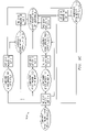
- FIGS. 9A–9G depict a section of code being operated upon by the embodiment of the invention in FIGS. 5A–5B .
- FIG. 9A depicts the intermediate code for a FIR filter kernel with 8 operations, including a branch OP 275 , two adds OP 62 OP 75 , one move OP 100 , two loads OP 107 OP 114 , a multiply-add OP 128 , and a store OP 153 .
- the notation var_num[ 1 ] is a reference to the variable from a prior iteration and will also cause data dependencies.
- FIG. 9B depicts a program graph 902 created by node 530 on code 901 .
- the USEs are listed on the first line
- the OP is listed on the second line
- the DEFs are listed on the third line.
- the widths of the operands are also provided.
- FIG. 9C depicts a model netlist 903 created by node 531 from program graph 902 .
- the weight e.g. area
- the operations that are part of the component For each net, the weight (e.g. width) is listed as well as the variables that are defined by the net.
- component 1003 has a weight of 152, was created from the add operation 75 , and is connected to net 102 that has a weight of 32 and was created from the variable 3 .
- FIG. 9D depicts a bi-partitioning 904 which is created by node 512 from model netlist 903 , assuming that no components were grouped by node 532 .
- Two partitions 905 and 906 are formed.
- the cutsize is the total weight of the nets cut by the partitioning.
- the nets that are cut by 905 and 906 are net 107 (weight 1), net 105 (weight 16), and net 106 (weight 16), yielding a cutsize of 33.
- FIG. 9E depicts the netlist after the group components node 532 .
- the resulting model netlist 907 is shown in FIG. 9E . Note that components 1005 and 1003 from model netlist 903 have been replaced by component 1009 in model netlist 907 .
- the weight of the new component 1009 is 304 , and it connects to nets 107 , 102 and 103 .
- FIG. 9F depicts a bi-partitioning 908 created by node 512 from model netlist 907 .
- Two partitions 909 and 910 are formed. Note that the two add operations 75 62 are now in the same partition 909 , whereas without the grouping step they were in different partitions as shown in FIG. 9D . Hence, the adds will be able to share the same hardware in partitioning 908 , whereas two adders would have been required for partitioning 904 . However, the cutsize of partitioning 908 has now increased to 57 (nets 107 , 102 , 104 , and 106 are cut with weights of 1, 32, 8, and 16 respectively) because of the grouping.
- FIG. 9G depicts the program graph 911 of the code formed by node 533 on the partitioning of 908 .
- the first form of compensation is the constraints on FU allocation and scheduling. The operations are grouped into partitions 912 and 913 . Functional unit allocation will occur on each partition independent of the other. In addition, scheduling will be constrained to only map operations to functional units from the corresponding partition.
- Another form of compensation is the MOVE operations. In this example, two move operations were added on each cut net. For example, the predicate variable 218 is moved from partition 912 to partition 913 via the predicate move operations OP 281 and OP 282 . Note that the fan-out of 218 has been reduced, which may reduce wire delay. In the original program graph 902 , the fan-out of variable 218 was 7.
- the fan-out of 218 is 5.
- the three other USEs of 218 in 902 are now driven by the new predicate variable 222 in 911 .
- the compensation causes the final netlist to have small sized sub-circuits. These can be identified as partitions 912 and 913 in FIG. 9G . Each of these partitions will have their own functional unit allocation, and hence will become their own sub-circuits. In addition, the moves between partitions will become registers, so backend physical design will have the flexibility of placing these partitions far apart while still meeting timing.
- the elements of the present invention are essentially the code segments to perform the necessary tasks.
- the program or code segments can be stored in a processor readable medium or transmitted by a computer data signal embodied in a carrier wave, or a signal modulated by a carrier, over a transmission medium.
- the “processor readable medium” may include any medium that can store or transfer information. Examples of the processor readable medium include an electronic circuit, a semiconductor memory device, a ROM, a flash memory, an erasable ROM (EROM), a floppy diskette, a compact disk CD-ROM, an optical disk, a hard disk, a fiber optic medium, a radio frequency (RF) link, etc.
- the computer data signal may include any signal that can propagate over a transmission medium such as electronic network channels, optical fibers, air, electromagnetic, RF links, etc.
- the code segments may be downloaded via computer networks such as the Internet, Intranet, etc.
- FIG. 8 illustrates computer system 800 adapted to use the present invention.
- Central processing unit (CPU) 801 is coupled to system bus 802 .
- the CPU 801 may be any general purpose CPU, such as an HP PA-8500 or Intel Pentium processor. However, the present invention is not restricted by the architecture of CPU 801 as long as CPU 801 supports the inventive operations as described herein.
- Bus 802 is coupled to random access memory (RAM) 803 , which may be SRAM, DRAM, or SDRAM.
- RAM 804 is also coupled to bus 802 , which may be PROM, EPROM, or EEPROM.
- RAM 803 and ROM 804 hold user and system data and programs as is well known in the art.
- Bus 802 is also coupled to input/output (I/O) controller card 805 , communications adapter card 811 , user interface card 808 , and display card 809 .
- the I/O adapter card 805 connects to storage devices 806 , such as one or more of a hard drive, a CD drive, a floppy disk drive, a tape drive, to the computer system.
- the I/O adapter 805 is also connected to printer 814 , which would allow the system to print paper copies of information such as document, photographs, articles, etc. Note that the printer may a printer (e.g. dot matrix, laser, etc.), a fax machine, or a copier machine.
- Communications card 811 is adapted to couple the computer system 800 to a network 812 , which may be one or more of a telephone network, a local (LAN) and/or a wide-area (WAN) network, an Ethernet network, and/or the Internet network.
- a network 812 may be one or more of a telephone network, a local (LAN) and/or a wide-area (WAN) network, an Ethernet network, and/or the Internet network.
- User interface card 808 couples user input devices, such as keyboard 813 , pointing device 807 , and microphone 816 , to the computer system 800 .
- User interface card 808 also provides sound output to a user via speaker(s) 815 .
- the display card 809 is driven by CPU 801 to control the display on display device 810 .
Abstract
Description
Claims (47)
Priority Applications (6)
| Application Number | Priority Date | Filing Date | Title |
|---|---|---|---|
| US10/266,719 US7107568B2 (en) | 2002-10-07 | 2002-10-07 | System and method for reducing wire delay or congestion during synthesis of hardware solvers |
| AU2003282708A AU2003282708A1 (en) | 2002-10-07 | 2003-10-03 | A system and method for reducing wire delay or congestion during synthesis of hardware solvers |
| EP03774593A EP1550059B1 (en) | 2002-10-07 | 2003-10-03 | A system and method for reducing wire delay or congestion during synthesis of hardware solvers |
| JP2004543399A JP2006502502A (en) | 2002-10-07 | 2003-10-03 | System and method for reducing wiring delay or congestion during hardware solver synthesis |
| PCT/US2003/031619 WO2004034291A2 (en) | 2002-10-07 | 2003-10-03 | A system and method for reducing wire delay or congestion during synthesis of hardware solvers |
| DE60318086T DE60318086T2 (en) | 2002-10-07 | 2003-10-03 | SYSTEM AND METHOD OF REDUCING LINE DELAY OR OVERLOAD IN SYNTHESIS OF HARDWARE SOLVERN |
Applications Claiming Priority (1)
| Application Number | Priority Date | Filing Date | Title |
|---|---|---|---|
| US10/266,719 US7107568B2 (en) | 2002-10-07 | 2002-10-07 | System and method for reducing wire delay or congestion during synthesis of hardware solvers |
Publications (2)
| Publication Number | Publication Date |
|---|---|
| US20040068331A1 US20040068331A1 (en) | 2004-04-08 |
| US7107568B2 true US7107568B2 (en) | 2006-09-12 |
Family
ID=32042713
Family Applications (1)
| Application Number | Title | Priority Date | Filing Date |
|---|---|---|---|
| US10/266,719 Active 2024-09-14 US7107568B2 (en) | 2002-10-07 | 2002-10-07 | System and method for reducing wire delay or congestion during synthesis of hardware solvers |
Country Status (6)
| Country | Link |
|---|---|
| US (1) | US7107568B2 (en) |
| EP (1) | EP1550059B1 (en) |
| JP (1) | JP2006502502A (en) |
| AU (1) | AU2003282708A1 (en) |
| DE (1) | DE60318086T2 (en) |
| WO (1) | WO2004034291A2 (en) |
Cited By (33)
| Publication number | Priority date | Publication date | Assignee | Title |
|---|---|---|---|---|
| US20070245272A1 (en) * | 2004-12-01 | 2007-10-18 | Andre Rohe | Concurrent optimization of physical design and operational cycle assignment |
| US20080307380A1 (en) * | 2004-12-01 | 2008-12-11 | Andre Rohe | Operational Cycle Assignment in a Configurable IC |
| US20090043620A1 (en) * | 2007-08-08 | 2009-02-12 | National Tsing Hua University | Method for copy propagations for a processor |
| US7669097B1 (en) | 2006-03-27 | 2010-02-23 | Tabula, Inc. | Configurable IC with error detection and correction circuitry |
| US20100050140A1 (en) * | 2008-08-25 | 2010-02-25 | Ali Corporation | Layout Method for a Chip |
| US7679401B1 (en) | 2005-12-01 | 2010-03-16 | Tabula, Inc. | User registers implemented with routing circuits in a configurable IC |
| US20100123133A1 (en) * | 2008-11-20 | 2010-05-20 | Joerg Wunderlich | Spin-polarised charge-carrier device |
| US20100125820A1 (en) * | 2008-11-14 | 2010-05-20 | Ispir Mustafa | Unfolding algorithm in multirate system folding |
| US7804730B2 (en) | 2005-03-15 | 2010-09-28 | Tabula, Inc. | Method and apparatus for accessing contents of memory cells |
| US7825685B2 (en) | 2007-09-06 | 2010-11-02 | Tabula, Inc. | Configuration context switcher with a clocked storage element |
| US7825687B2 (en) | 2004-11-08 | 2010-11-02 | Tabula, Inc. | Storage elements for a configurable IC and method and apparatus for accessing data stored in the storage elements |
| US7873934B1 (en) * | 2007-11-23 | 2011-01-18 | Altera Corporation | Method and apparatus for implementing carry chains on field programmable gate array devices |
| US7872496B2 (en) | 2004-02-14 | 2011-01-18 | Tabula, Inc. | Method of mapping a user design defined for a user design cycle to an IC with multiple sub-cycle reconfigurable circuits |
| US7898291B2 (en) | 2004-12-01 | 2011-03-01 | Tabula, Inc. | Operational time extension |
| US7926016B1 (en) * | 2005-09-30 | 2011-04-12 | Xilinx, Inc. | Timing driven logic block configuration |
| US7948266B2 (en) | 2004-02-14 | 2011-05-24 | Tabula, Inc. | Non-sequentially configurable IC |
| US7971172B1 (en) | 2005-11-07 | 2011-06-28 | Tabula, Inc. | IC that efficiently replicates a function to save logic and routing resources |
| US8093922B2 (en) | 2007-03-20 | 2012-01-10 | Tabula, Inc. | Configurable IC having a routing fabric with storage elements |
| US8112468B1 (en) | 2007-03-22 | 2012-02-07 | Tabula, Inc. | Method and apparatus for performing an operation with a plurality of sub-operations in a configurable IC |
| US8166435B2 (en) | 2008-06-26 | 2012-04-24 | Tabula, Inc. | Timing operations in an IC with configurable circuits |
| US8183882B2 (en) | 2004-11-08 | 2012-05-22 | Tabula, Inc. | Reconfigurable IC that has sections running at different reconfiguration rates |
| US8468476B1 (en) * | 2007-11-23 | 2013-06-18 | Altera Corporation | Method and apparatus for designing a system on multiple field programmable gate array device types |
| US8495535B2 (en) | 2011-11-28 | 2013-07-23 | International Business Machines Corporation | Partitioning and scheduling uniform operator logic trees for hardware accelerators |
| US8595688B1 (en) * | 2003-09-08 | 2013-11-26 | Synopsys, Inc. | Generation of instruction set from architecture description |
| US8789001B1 (en) | 2013-02-20 | 2014-07-22 | Tabula, Inc. | System and method for using fabric-graph flow to determine resource costs |
| US8806404B2 (en) | 2010-04-02 | 2014-08-12 | Tabula, Inc. | System and method for reducing reconfiguration power usage |
| US8832618B1 (en) * | 2009-10-01 | 2014-09-09 | Altera Corporation | Method and apparatus for automatic hierarchical design partitioning |
| US8863067B1 (en) | 2008-02-06 | 2014-10-14 | Tabula, Inc. | Sequential delay analysis by placement engines |
| US8935647B2 (en) | 2008-05-24 | 2015-01-13 | Tabula, Inc. | Decision modules |
| US8984464B1 (en) | 2011-11-21 | 2015-03-17 | Tabula, Inc. | Detailed placement with search and repair |
| US20150286761A1 (en) * | 2012-06-01 | 2015-10-08 | Flexras Technologies | Multi-fpga prototyping of an asic circuit |
| US20160070849A1 (en) * | 2014-09-09 | 2016-03-10 | International Business Machines Corporation | Critical region identification |
| US9971858B1 (en) * | 2015-02-20 | 2018-05-15 | Altera Corporation | Method and apparatus for performing register retiming in the presence of false path timing analysis exceptions |
Families Citing this family (25)
| Publication number | Priority date | Publication date | Assignee | Title |
|---|---|---|---|---|
| US6952816B2 (en) * | 2002-10-07 | 2005-10-04 | Hewlett-Packard Development Company, L.P. | Methods and apparatus for digital circuit design generation |
| US7096438B2 (en) * | 2002-10-07 | 2006-08-22 | Hewlett-Packard Development Company, L.P. | Method of using clock cycle-time in determining loop schedules during circuit design |
| US7000137B2 (en) * | 2002-10-07 | 2006-02-14 | Hewlett-Packard Development Company, L.P. | System for and method of clock cycle-time analysis using mode-slicing mechanism |
| US7237214B1 (en) * | 2003-03-04 | 2007-06-26 | Synplicity, Inc. | Method and apparatus for circuit partitioning and trace assignment in circuit design |
| US7324512B2 (en) * | 2003-06-12 | 2008-01-29 | International Business Machines Corporation | MAC layer bridging of network frames between isolated and external networks |
| US7373615B2 (en) * | 2004-02-17 | 2008-05-13 | International Business Machines Corporation | Method for optimization of logic circuits for routability |
| US8595674B2 (en) * | 2007-07-23 | 2013-11-26 | Synopsys, Inc. | Architectural physical synthesis |
| US8661380B1 (en) * | 2008-02-19 | 2014-02-25 | Altera Corporation | Method and apparatus for performing parallel synthesis on a field programmable gate array |
| US8661381B1 (en) | 2008-05-15 | 2014-02-25 | Altera Corporation | Method and apparatus for performing optimization using Don't Care states |
| US9230047B1 (en) * | 2010-06-11 | 2016-01-05 | Altera Corporation | Method and apparatus for partitioning a synthesis netlist for compile time and quality of results improvement |
| ES2642964T3 (en) | 2012-03-19 | 2017-11-20 | Massachusetts Institute Of Technology | Variable impedance mechanical interface |
| US8762909B1 (en) * | 2013-03-12 | 2014-06-24 | Avago Technologies General Ip (Singapore) Pte. Ltd. | System and method for automatic timing-based register placement and register location adjustment in an integrated circuit (IC) |
| JP6398729B2 (en) * | 2015-01-08 | 2018-10-03 | 株式会社ソシオネクスト | Design support apparatus and design support method |
| US10191948B2 (en) * | 2015-02-27 | 2019-01-29 | Microsoft Technology Licensing, Llc | Joins and aggregations on massive graphs using large-scale graph processing |
| US9824177B1 (en) | 2016-03-24 | 2017-11-21 | Altera Corporation | Method and apparatus for verifying structural correctness in retimed circuits |
| US10157247B2 (en) | 2016-03-24 | 2018-12-18 | Intel Corporation | Method and apparatus for performing rewind structural verification of retimed circuits driven by a plurality of clocks |
| US10706203B1 (en) * | 2016-03-24 | 2020-07-07 | Altera Corporation | Method and apparatus for verifying initial state equivalence of changed registers in retimed circuits |
| US10417374B1 (en) * | 2016-05-09 | 2019-09-17 | Altera Corporation | Method and apparatus for performing register retiming by utilizing native timing-driven constraints |
| CN106249519A (en) * | 2016-08-22 | 2016-12-21 | 深圳市华星光电技术有限公司 | A kind of projector |
| US10769008B1 (en) * | 2016-12-06 | 2020-09-08 | Cadence Design Systems, Inc. | Systems and methods for automatic formal metastability fault analysis in an electronic design |
| US10671398B2 (en) * | 2017-08-02 | 2020-06-02 | International Business Machines Corporation | Low-overhead, low-latency operand dependency tracking for instructions operating on register pairs in a processor core |
| US11106968B1 (en) * | 2018-05-24 | 2021-08-31 | Xilinx, Inc. | Circuit arrangements and methods for traversing input feature maps |
| US11403254B2 (en) | 2018-08-16 | 2022-08-02 | Tachyum Ltd. | System and method for populating multiple instruction words |
| CN113918133B (en) * | 2021-12-14 | 2022-02-25 | 武汉鼎元同立科技有限公司 | Optimal control problem solver construction method and system |
| KR102454202B1 (en) * | 2022-05-04 | 2022-10-17 | 주식회사 애자일소다 | System and method for designing integrated circuits based on deep reinforcement learning using partitioning |
Citations (15)
| Publication number | Priority date | Publication date | Assignee | Title |
|---|---|---|---|---|
| US6075935A (en) | 1997-12-01 | 2000-06-13 | Improv Systems, Inc. | Method of generating application specific integrated circuits using a programmable hardware architecture |
| US6226776B1 (en) * | 1997-09-16 | 2001-05-01 | Synetry Corporation | System for converting hardware designs in high-level programming language to hardware implementations |
| US20010016936A1 (en) * | 2000-02-18 | 2001-08-23 | Kazuhisa Okada | High- level synthesis method and storage medium storing the same |
| US6314552B1 (en) * | 1998-05-18 | 2001-11-06 | Lev A. Markov | Electronic design creation through architectural exploration |
| US6397341B1 (en) * | 1999-08-27 | 2002-05-28 | Synopsys, Inc. | Method for improving the speed of behavioral synthesis links to logic synthesis |
| US6438739B1 (en) | 1997-12-22 | 2002-08-20 | Sharp Kabushiki Kaisha | High-level synthesis device high level synthesis method and recording medium with high level synthesis program |
| US20020138816A1 (en) | 1998-06-12 | 2002-09-26 | Majid Sarrafzadeh | Placement method for integrated circuit design using topo-clustering |
| US20020188923A1 (en) * | 2001-06-11 | 2002-12-12 | Mitsuhisa Ohnishi | High-level synthesis apparatus, high-level synthesis method, method for producing logic circuit using the high-level synthesis method, and recording medium |
| US6557158B1 (en) * | 1999-06-03 | 2003-04-29 | Sharp Kabushiki Kaisha | Scheduling method for high-level synthesis and recording medium |
| US6625797B1 (en) * | 2000-02-10 | 2003-09-23 | Xilinx, Inc. | Means and method for compiling high level software languages into algorithmically equivalent hardware representations |
| US20040068711A1 (en) * | 2002-10-07 | 2004-04-08 | Shail-Aditya Gupta | Digital circuit synthesis including timing convergence and routability |
| US6782511B1 (en) * | 1999-05-26 | 2004-08-24 | Cadence Design Systems, Inc. | Behavioral-synthesis electronic design automation tool business-to-business application service provider |
| US6829756B1 (en) * | 2002-09-23 | 2004-12-07 | Xilinx, Inc. | Programmable logic device with time-multiplexed interconnect |
| US6925628B2 (en) * | 2002-10-22 | 2005-08-02 | Matsushita Electric Industrial Co., Ltd. | High-level synthesis method |
| US6941541B2 (en) * | 2002-07-19 | 2005-09-06 | Hewlett-Packard Development Company, L.P. | Efficient pipelining of synthesized synchronous circuits |
-
2002
- 2002-10-07 US US10/266,719 patent/US7107568B2/en active Active
-
2003
- 2003-10-03 JP JP2004543399A patent/JP2006502502A/en active Pending
- 2003-10-03 DE DE60318086T patent/DE60318086T2/en not_active Expired - Lifetime
- 2003-10-03 WO PCT/US2003/031619 patent/WO2004034291A2/en active IP Right Grant
- 2003-10-03 EP EP03774593A patent/EP1550059B1/en not_active Expired - Fee Related
- 2003-10-03 AU AU2003282708A patent/AU2003282708A1/en not_active Abandoned
Patent Citations (18)
| Publication number | Priority date | Publication date | Assignee | Title |
|---|---|---|---|---|
| US6226776B1 (en) * | 1997-09-16 | 2001-05-01 | Synetry Corporation | System for converting hardware designs in high-level programming language to hardware implementations |
| US6848085B2 (en) * | 1997-09-16 | 2005-01-25 | Synopsys, Inc. | System for converting hardware designs in high-level programming languages to hardware implementations |
| US20010034876A1 (en) * | 1997-09-16 | 2001-10-25 | Synetry Corporation | System for converting hardware designs in high-level programming languages to hardware implementations |
| US6075935A (en) | 1997-12-01 | 2000-06-13 | Improv Systems, Inc. | Method of generating application specific integrated circuits using a programmable hardware architecture |
| US6438739B1 (en) | 1997-12-22 | 2002-08-20 | Sharp Kabushiki Kaisha | High-level synthesis device high level synthesis method and recording medium with high level synthesis program |
| US6314552B1 (en) * | 1998-05-18 | 2001-11-06 | Lev A. Markov | Electronic design creation through architectural exploration |
| US20020138816A1 (en) | 1998-06-12 | 2002-09-26 | Majid Sarrafzadeh | Placement method for integrated circuit design using topo-clustering |
| US6782511B1 (en) * | 1999-05-26 | 2004-08-24 | Cadence Design Systems, Inc. | Behavioral-synthesis electronic design automation tool business-to-business application service provider |
| US6557158B1 (en) * | 1999-06-03 | 2003-04-29 | Sharp Kabushiki Kaisha | Scheduling method for high-level synthesis and recording medium |
| US6397341B1 (en) * | 1999-08-27 | 2002-05-28 | Synopsys, Inc. | Method for improving the speed of behavioral synthesis links to logic synthesis |
| US6625797B1 (en) * | 2000-02-10 | 2003-09-23 | Xilinx, Inc. | Means and method for compiling high level software languages into algorithmically equivalent hardware representations |
| US20010016936A1 (en) * | 2000-02-18 | 2001-08-23 | Kazuhisa Okada | High- level synthesis method and storage medium storing the same |
| US20020188923A1 (en) * | 2001-06-11 | 2002-12-12 | Mitsuhisa Ohnishi | High-level synthesis apparatus, high-level synthesis method, method for producing logic circuit using the high-level synthesis method, and recording medium |
| US6941541B2 (en) * | 2002-07-19 | 2005-09-06 | Hewlett-Packard Development Company, L.P. | Efficient pipelining of synthesized synchronous circuits |
| US6829756B1 (en) * | 2002-09-23 | 2004-12-07 | Xilinx, Inc. | Programmable logic device with time-multiplexed interconnect |
| US20040068711A1 (en) * | 2002-10-07 | 2004-04-08 | Shail-Aditya Gupta | Digital circuit synthesis including timing convergence and routability |
| US6952816B2 (en) * | 2002-10-07 | 2005-10-04 | Hewlett-Packard Development Company, L.P. | Methods and apparatus for digital circuit design generation |
| US6925628B2 (en) * | 2002-10-22 | 2005-08-02 | Matsushita Electric Industrial Co., Ltd. | High-level synthesis method |
Non-Patent Citations (5)
| Title |
|---|
| J H Panner et al-"A 300 K-Circuit ASIC Logic Family CAD System"-IEEE Custom Integrated Circuit Conference-May 13, 1990-pp. 10.4.1-10.4.5. |
| Moonwook Oh et el-"Rate Optimal VLSI Design From Data Flow Graph"-Desgin Automation Conference Proceedings-Jun. 15. 1998-pp. 118-121. |
| S Bara et al-"Ultra-Fast Poisson's Equation Solvers Using Wired-Up Processors for Virtual Devices Architectures"-Proceedings Semiconductor Conference-Oct. 1999-pp. 249-252. |
| S, Dey et al-"Exploiting Hardware Sharing in High-Level Synthesis for Partial Scan Optimization"-IEEE/ACM Int'l Conferencer on Computer Aided Design-Nov. 11, 1993-Conf 11-pp. 20-25. |
| Terry Tao Ye et al-"Data Path Placement With Regularity"-IEEE/ACM Int'l Conference on Computer-Aided Design-Nov. 5, 2000 pp. 264-270. |
Cited By (71)
| Publication number | Priority date | Publication date | Assignee | Title |
|---|---|---|---|---|
| US9317298B2 (en) * | 2003-09-08 | 2016-04-19 | Synopsys, Inc. | Generation of instruction set from architecture description |
| US20140109040A1 (en) * | 2003-09-08 | 2014-04-17 | Synopsys, Inc. | Generation of Instruction Set from Architecture Description |
| US8595688B1 (en) * | 2003-09-08 | 2013-11-26 | Synopsys, Inc. | Generation of instruction set from architecture description |
| US8305110B2 (en) | 2004-02-14 | 2012-11-06 | Tabula, Inc. | Non-sequentially configurable IC |
| US8193830B2 (en) | 2004-02-14 | 2012-06-05 | Tabula, Inc. | Configurable circuits, IC's, and systems |
| US7948266B2 (en) | 2004-02-14 | 2011-05-24 | Tabula, Inc. | Non-sequentially configurable IC |
| US7872496B2 (en) | 2004-02-14 | 2011-01-18 | Tabula, Inc. | Method of mapping a user design defined for a user design cycle to an IC with multiple sub-cycle reconfigurable circuits |
| US7825687B2 (en) | 2004-11-08 | 2010-11-02 | Tabula, Inc. | Storage elements for a configurable IC and method and apparatus for accessing data stored in the storage elements |
| US8183882B2 (en) | 2004-11-08 | 2012-05-22 | Tabula, Inc. | Reconfigurable IC that has sections running at different reconfiguration rates |
| US8159264B2 (en) | 2004-11-08 | 2012-04-17 | Tabula, Inc. | Storage elements for a configurable IC and method and apparatus for accessing data stored in the storage elements |
| US7898291B2 (en) | 2004-12-01 | 2011-03-01 | Tabula, Inc. | Operational time extension |
| US20110145776A1 (en) * | 2004-12-01 | 2011-06-16 | Andre Rohe | Operational cycle assignment in a configurable ic |
| US20080307380A1 (en) * | 2004-12-01 | 2008-12-11 | Andre Rohe | Operational Cycle Assignment in a Configurable IC |
| US20080307378A1 (en) * | 2004-12-01 | 2008-12-11 | Andre Rohe | Operational Cycle Assignment in a Configurable IC |
| US7870530B2 (en) | 2004-12-01 | 2011-01-11 | Tabula, Inc. | Operational cycle assignment in a configurable IC |
| US7870529B2 (en) | 2004-12-01 | 2011-01-11 | Tabula, Inc. | Operational cycle assignment in a configurable IC |
| US8683410B2 (en) | 2004-12-01 | 2014-03-25 | Tabula, Inc. | Operational cycle assignment in a configurable IC |
| US8664974B2 (en) | 2004-12-01 | 2014-03-04 | Tabula, Inc. | Operational time extension |
| US20070245272A1 (en) * | 2004-12-01 | 2007-10-18 | Andre Rohe | Concurrent optimization of physical design and operational cycle assignment |
| US7694265B2 (en) | 2004-12-01 | 2010-04-06 | Tabula, Inc. | Operational cycle assignment in a configurable IC |
| US7496879B2 (en) * | 2004-12-01 | 2009-02-24 | Tabula, Inc. | Concurrent optimization of physical design and operational cycle assignment |
| US7804730B2 (en) | 2005-03-15 | 2010-09-28 | Tabula, Inc. | Method and apparatus for accessing contents of memory cells |
| US7926016B1 (en) * | 2005-09-30 | 2011-04-12 | Xilinx, Inc. | Timing driven logic block configuration |
| US7971172B1 (en) | 2005-11-07 | 2011-06-28 | Tabula, Inc. | IC that efficiently replicates a function to save logic and routing resources |
| US7679401B1 (en) | 2005-12-01 | 2010-03-16 | Tabula, Inc. | User registers implemented with routing circuits in a configurable IC |
| US8089300B2 (en) | 2005-12-01 | 2012-01-03 | Tabula, Inc. | Users registers implemented with routing circuits in a configurable IC |
| US7669097B1 (en) | 2006-03-27 | 2010-02-23 | Tabula, Inc. | Configurable IC with error detection and correction circuitry |
| US8093922B2 (en) | 2007-03-20 | 2012-01-10 | Tabula, Inc. | Configurable IC having a routing fabric with storage elements |
| US8112468B1 (en) | 2007-03-22 | 2012-02-07 | Tabula, Inc. | Method and apparatus for performing an operation with a plurality of sub-operations in a configurable IC |
| US20090043620A1 (en) * | 2007-08-08 | 2009-02-12 | National Tsing Hua University | Method for copy propagations for a processor |
| US8051411B2 (en) * | 2007-08-08 | 2011-11-01 | National Tsing Hua University | Method for copy propagations for a processor with distributed register file design |
| US7825685B2 (en) | 2007-09-06 | 2010-11-02 | Tabula, Inc. | Configuration context switcher with a clocked storage element |
| US8248101B2 (en) | 2007-09-06 | 2012-08-21 | Tabula, Inc. | Reading configuration data from internal storage node of configuration storage circuit |
| US7928761B2 (en) | 2007-09-06 | 2011-04-19 | Tabula, Inc. | Configuration context switcher with a latch |
| US8324931B2 (en) | 2007-09-06 | 2012-12-04 | Tabula, Inc. | Configuration context switcher with a latch |
| US8344755B2 (en) | 2007-09-06 | 2013-01-01 | Tabula, Inc. | Configuration context switcher |
| US8138789B2 (en) | 2007-09-06 | 2012-03-20 | Tabula, Inc. | Configuration context switcher with a clocked storage element |
| US7873934B1 (en) * | 2007-11-23 | 2011-01-18 | Altera Corporation | Method and apparatus for implementing carry chains on field programmable gate array devices |
| US9026967B1 (en) | 2007-11-23 | 2015-05-05 | Altera Corporation | Method and apparatus for designing a system on multiple field programmable gate array device types |
| US8793629B1 (en) | 2007-11-23 | 2014-07-29 | Altera Corporation | Method and apparatus for implementing carry chains on FPGA devices |
| US8468476B1 (en) * | 2007-11-23 | 2013-06-18 | Altera Corporation | Method and apparatus for designing a system on multiple field programmable gate array device types |
| US8739102B1 (en) | 2007-11-23 | 2014-05-27 | Altera Corporation | Method and apparatus for designing a system on multiple field programmable gate array device types |
| US8863067B1 (en) | 2008-02-06 | 2014-10-14 | Tabula, Inc. | Sequential delay analysis by placement engines |
| US8935647B2 (en) | 2008-05-24 | 2015-01-13 | Tabula, Inc. | Decision modules |
| US8756547B2 (en) | 2008-06-26 | 2014-06-17 | Tabula, Inc. | Timing operations in an IC with configurable circuits |
| US8166435B2 (en) | 2008-06-26 | 2012-04-24 | Tabula, Inc. | Timing operations in an IC with configurable circuits |
| US20100050140A1 (en) * | 2008-08-25 | 2010-02-25 | Ali Corporation | Layout Method for a Chip |
| US7926017B2 (en) * | 2008-08-25 | 2011-04-12 | Ali Corporation | Layout method for a chip |
| US20100125820A1 (en) * | 2008-11-14 | 2010-05-20 | Ispir Mustafa | Unfolding algorithm in multirate system folding |
| US8136063B2 (en) * | 2008-11-14 | 2012-03-13 | Synopsys, Inc. | Unfolding algorithm in multirate system folding |
| US20100123133A1 (en) * | 2008-11-20 | 2010-05-20 | Joerg Wunderlich | Spin-polarised charge-carrier device |
| US10339243B2 (en) * | 2009-10-01 | 2019-07-02 | Altera Corporation | Method and apparatus for automatic hierarchical design partitioning |
| US8832618B1 (en) * | 2009-10-01 | 2014-09-09 | Altera Corporation | Method and apparatus for automatic hierarchical design partitioning |
| US20180189427A1 (en) * | 2009-10-01 | 2018-07-05 | Altera Corporation | Method and apparatus for automatic hierarchical design partitioning |
| US9922156B1 (en) * | 2009-10-01 | 2018-03-20 | Altera Corporation | Method and apparatus for automatic hierarchical design partitioning |
| US8806404B2 (en) | 2010-04-02 | 2014-08-12 | Tabula, Inc. | System and method for reducing reconfiguration power usage |
| US9143128B2 (en) | 2010-04-02 | 2015-09-22 | Altera Coporation | System and method for reducing reconfiguration power usage |
| US8984464B1 (en) | 2011-11-21 | 2015-03-17 | Tabula, Inc. | Detailed placement with search and repair |
| US8495535B2 (en) | 2011-11-28 | 2013-07-23 | International Business Machines Corporation | Partitioning and scheduling uniform operator logic trees for hardware accelerators |
| US9400860B2 (en) * | 2012-06-01 | 2016-07-26 | Mentor Graphics Corporation | Multi-FPGA prototyping of an ASIC circuit |
| US9817934B2 (en) | 2012-06-01 | 2017-11-14 | Mentor Graphics Corporation | Multi-FPGA prototyping of an ASIC circuit |
| US20150286761A1 (en) * | 2012-06-01 | 2015-10-08 | Flexras Technologies | Multi-fpga prototyping of an asic circuit |
| US9047431B2 (en) | 2013-02-20 | 2015-06-02 | Tabula, Inc. | System and method for using fabric-graph flow to determine resource costs |
| US8789001B1 (en) | 2013-02-20 | 2014-07-22 | Tabula, Inc. | System and method for using fabric-graph flow to determine resource costs |
| US20160070849A1 (en) * | 2014-09-09 | 2016-03-10 | International Business Machines Corporation | Critical region identification |
| US9378326B2 (en) * | 2014-09-09 | 2016-06-28 | International Business Machines Corporation | Critical region identification |
| US20160217248A1 (en) * | 2014-09-09 | 2016-07-28 | International Business Machines Corporation | Critical region identification |
| US9659140B2 (en) * | 2014-09-09 | 2017-05-23 | International Business Machines Corporation | Critical region identification |
| US10140414B2 (en) * | 2014-09-09 | 2018-11-27 | International Business Machines Corporation | Critical region identification |
| US9971858B1 (en) * | 2015-02-20 | 2018-05-15 | Altera Corporation | Method and apparatus for performing register retiming in the presence of false path timing analysis exceptions |
| US10671781B2 (en) | 2015-02-20 | 2020-06-02 | Altera Corporation | Method and apparatus for performing register retiming in the presence of false path timing analysis exceptions |
Also Published As
| Publication number | Publication date |
|---|---|
| EP1550059A2 (en) | 2005-07-06 |
| AU2003282708A1 (en) | 2004-05-04 |
| DE60318086D1 (en) | 2008-01-24 |
| WO2004034291A2 (en) | 2004-04-22 |
| WO2004034291A3 (en) | 2004-07-22 |
| AU2003282708A8 (en) | 2004-05-04 |
| US20040068331A1 (en) | 2004-04-08 |
| DE60318086T2 (en) | 2008-12-04 |
| WO2004034291A9 (en) | 2006-05-26 |
| EP1550059B1 (en) | 2007-12-12 |
| JP2006502502A (en) | 2006-01-19 |
Similar Documents
| Publication | Publication Date | Title |
|---|---|---|
| US7107568B2 (en) | System and method for reducing wire delay or congestion during synthesis of hardware solvers | |
| US6952816B2 (en) | Methods and apparatus for digital circuit design generation | |
| Wei et al. | TGPA: tile-grained pipeline architecture for low latency CNN inference | |
| US11755810B2 (en) | Method and apparatus for performing parallel routing using a multi-threaded routing procedure | |
| US6493863B1 (en) | Method of designing semiconductor integrated circuit | |
| JP5706689B2 (en) | Architectural physical synthesis | |
| US9922156B1 (en) | Method and apparatus for automatic hierarchical design partitioning | |
| US7290239B1 (en) | Method and apparatus for performing post-placement functional decomposition for field programmable gate arrays | |
| Ly et al. | A generalized interconnect model for data path synthesis | |
| Chen et al. | MULTIPAR: Behavioral partition for synthesizing multiprocessor architectures | |
| US7689940B2 (en) | Method and apparatus for allocating data paths | |
| Sambhus | Reuse-Aware Temporal Partitioning of Data-Flow Graphs on a Coarse-Grained Reconfigurable Array | |
| US11507723B2 (en) | Method and apparatus for performing incremental compilation using structural netlist comparison | |
| Thepayasuwan et al. | Hardware-software co-design of resource constrained systems on a chip | |
| Hannig et al. | Parallelization approaches for hardware accelerators–loop unrolling versus loop partitioning | |
| Kim et al. | Parallelizing post-placement timing optimization | |
| Dai et al. | HETA: A Heterogeneous Temporal CGRA Modeling and Design Space Exploration via Bayesian Optimization | |
| Jones et al. | Tools for mapping applications to CCMs | |
| Ahmadinia | Concepts of Operating Systems for Reconfigurable Systems | |
| Geurts et al. | The High-Level Data-Path Mapping Script | |
| Geurts et al. | Operation Clustering |
Legal Events
| Date | Code | Title | Description |
|---|---|---|---|
| AS | Assignment |
Owner name: HEWLETT-PACKARD COMPANY, COLORADO Free format text: ASSIGNMENT OF ASSIGNORS INTEREST;ASSIGNOR:CRONQUIST, DARREN C.;REEL/FRAME:013428/0821 Effective date: 20021121 |
|
| AS | Assignment |
Owner name: HEWLETT-PACKARD DEVELOPMENT COMPANY, L.P., COLORAD Free format text: ASSIGNMENT OF ASSIGNORS INTEREST;ASSIGNOR:HEWLETT-PACKARD COMPANY;REEL/FRAME:013776/0928 Effective date: 20030131 Owner name: HEWLETT-PACKARD DEVELOPMENT COMPANY, L.P.,COLORADO Free format text: ASSIGNMENT OF ASSIGNORS INTEREST;ASSIGNOR:HEWLETT-PACKARD COMPANY;REEL/FRAME:013776/0928 Effective date: 20030131 |
|
| STCF | Information on status: patent grant |
Free format text: PATENTED CASE |
|
| FPAY | Fee payment |
Year of fee payment: 4 |
|
| AS | Assignment |
Owner name: SAMSUNG ELECTRONICS CO., LTD., KOREA, REPUBLIC OF Free format text: ASSIGNMENT OF ASSIGNORS INTEREST;ASSIGNORS:HEWLETT-PACKARD DEVELOPMENT COMPANY, L.P.;HEWLETT-PACKARD COMPANY;REEL/FRAME:026198/0139 Effective date: 20101019 |
|
| FPAY | Fee payment |
Year of fee payment: 8 |
|
| MAFP | Maintenance fee payment |
Free format text: PAYMENT OF MAINTENANCE FEE, 12TH YEAR, LARGE ENTITY (ORIGINAL EVENT CODE: M1553) Year of fee payment: 12 |